OPC+ Cloud PlatformOPC+ 光學鄰近修正平臺
Cloud-based freeform mask correction · GPU-accelerated OPC for semiconductor & photonics
雲端自由曲線光罩修正 · 以 GPU 加速的半導體與光子元件 OPC
Developed by PAL Lab & NSL Lab · National Yang Ming Chiao Tung University

What is Optical Proximity Correction (OPC)?什麼是光學鄰近修正(OPC)?
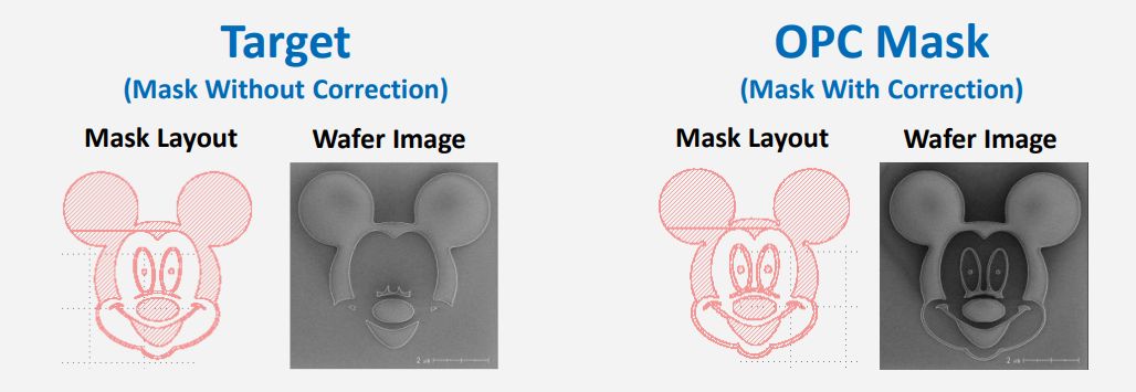
Chips and photonic devices are printed by projecting light through a mask onto a wafer: photolithography [1]. When features are as small as the light’s wavelength, diffraction blurs the image: line ends shorten, corners round and small features may not print at all.
晶片與光子元件是將光線透過光罩投影到晶圓上印製而成,稱為光學微影 [1]。當特徵尺寸小到與光的波長相當時,繞射會讓影像模糊:線端縮短、轉角變圓,細小的特徵甚至印不出來。
Optical Proximity Correction (OPC) pre-distorts the mask so the printed pattern matches the design; Inverse Lithography Technology (ILT) computes the whole mask shape directly from the target [2].
光學鄰近修正(OPC)預先修改光罩形狀,讓印出的圖案符合設計;反向微影技術(ILT)則直接由目標圖案求出整片光罩的形狀 [2]。
Why is traditional OPC insufficient?傳統 OPC 為何不足?
Conventional CPU-based, rule-driven tools take hours on large layouts, are costly to license and run, and handle only Manhattan (rectilinear) shapes, while photonics and curvilinear nodes need freeform masks.
傳統以 CPU、規則為基礎的工具處理大型版圖需要數小時,授權與操作成本高昂,而且只能處理曼哈頓(直線)形狀;光子元件與曲邊型製程卻需要自由曲線的光罩。
SEM validation on fabricated devices實際製作元件的 SEM 驗證
Scanning electron microscope (SEM) images of devices made at partner fabs, without and with OPC.
合作製程單位實際製作元件的掃描式電子顯微鏡(SEM)影像,比較未經與經過 OPC 修正的結果。
Line pattern — line-end shortening線條圖案 — 線端縮短
Without OPC, line ends pull back and print short; OPC extends the mask at the ends so the lines print at full length.
未經 OPC 時,線端向內退縮、線條印得太短;OPC 延長光罩上的線端,使線條印出完整長度。
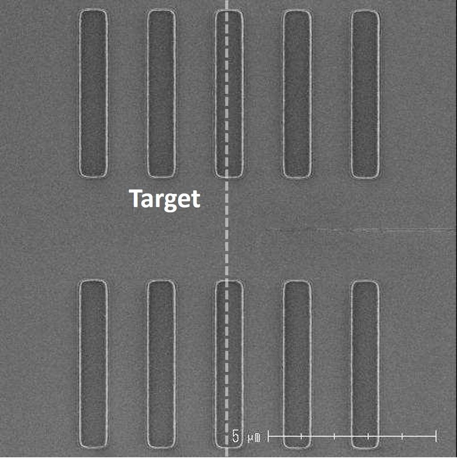
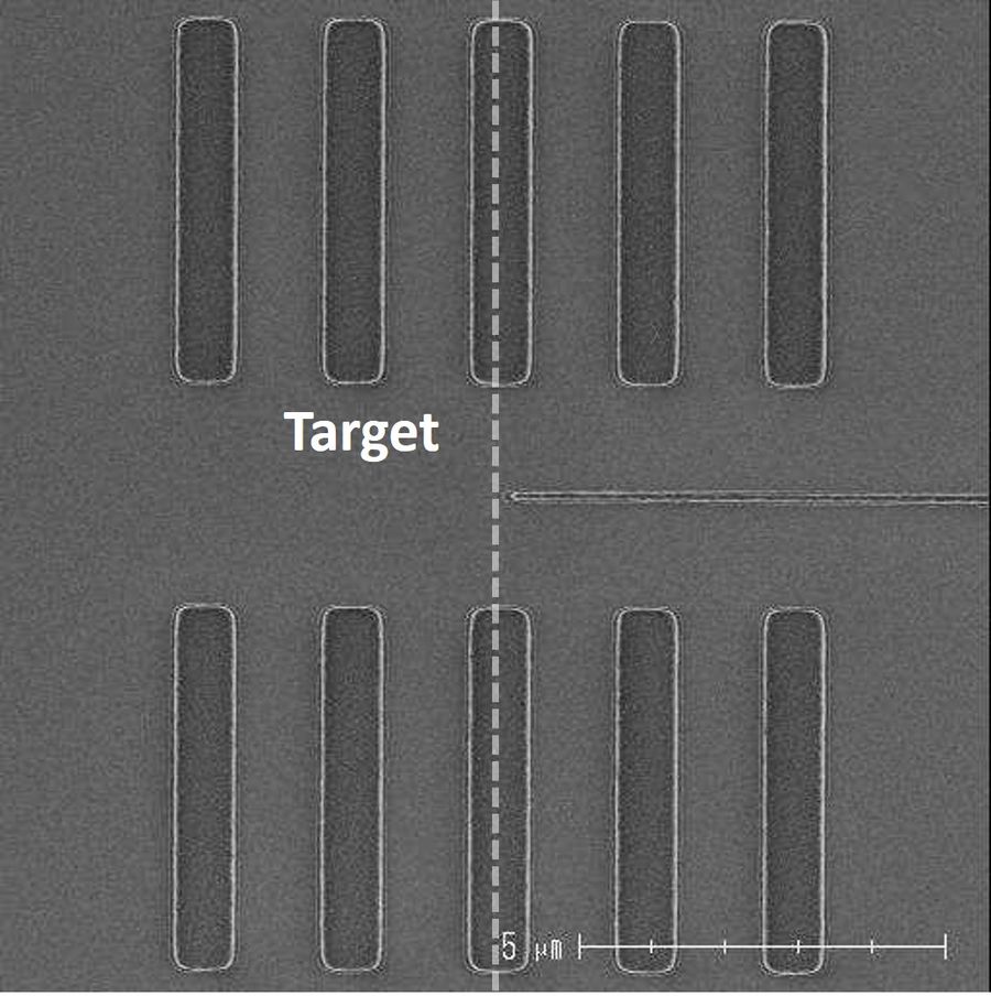
Figure 2. Line patterns. Scale bar: 5 µm.圖 2. 線條圖案。比例尺:5 µm。
Ring resonator — critical defect elimination環形共振器 — 消除致命缺陷
Without OPC, the coupling gap does not open and the ring does not work; with OPC, the gap is fully resolved [5].
未經 OPC 時,耦合間隙無法打開,元件無法運作;經 OPC 修正後,間隙完整解析 [5]。
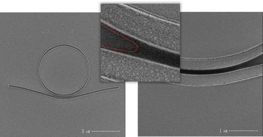
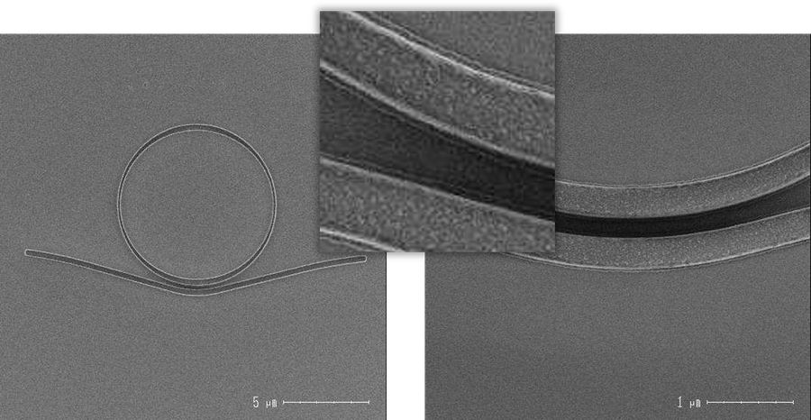
Figure 3. Ring resonators. Scale bar: 5 µm (overview), 1 µm (inset).圖 3. 環形共振器。比例尺:5 µm(全圖)、1 µm(插圖)。
Metalens — sub-wavelength feature survival超穎透鏡 — 次波長特徵的保留
Without OPC, the smallest sub-wavelength structures distort or vanish; with OPC, all of them survive and the lens keeps its phase profile [5].
未經 OPC 時,最小的次波長結構會變形或消失;經 OPC 修正後全部保留,透鏡維持預期的相位分佈 [5]。
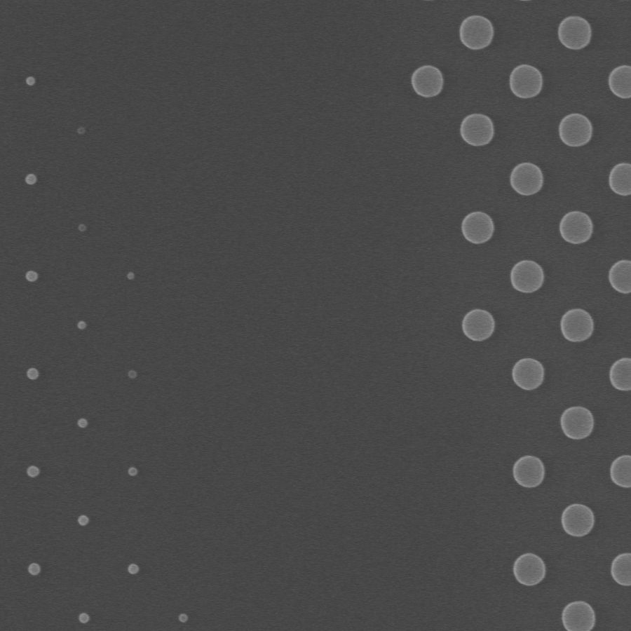
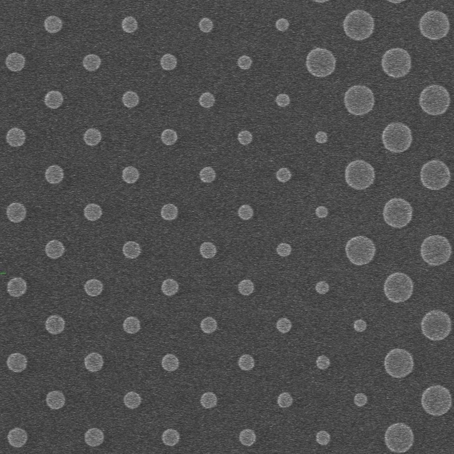
Figure 4. Metalens structures.圖 4. 超穎透鏡結構。
Key features主要特色
GPU accelerationGPU 加速
CUDA multi-stream parallelism corrects large layouts in minutes instead of hours [3][4].
CUDA 多串流平行運算,讓大型版圖的修正從數小時縮短到數分鐘 [3][4]。
Runs in your browser在瀏覽器中執行
Upload, set the scanner and submit: no scripting and no hardware to buy.
上傳、設定曝光機、送出即可:不需撰寫腳本,也無需購買硬體。
Native curvilinear masks原生曲邊型光罩
Curvilinear masks without polygon approximation keep the optical phase and waveguide coupling intact [5].
產生曲邊型光罩、無需多邊形近似,保留光學相位與波導耦合效率 [5]。
Global inverse optimization全域反向最佳化
Full-mask ILT with contour-based L2 optimization gives better pattern fidelity and CD uniformity than rule-based windowed correction [4][6].
以輪廓為基礎的 L2 全光罩 ILT 最佳化,圖案保真度與 CD 均勻度優於規則式的視窗修正 [4][6]。
Predictable turnaround可預測的週轉時間
Two-tier scheduling balances the work across mixed GPU nodes, so delivery times stay steady [3].
兩層式排程在異質 GPU 節點間平衡工作量,交付時間穩定 [3]。
Industry-standard formats業界標準格式
GDSII/OASIS layouts and CD-SEM calibration data fit your existing EDA flow.
支援 GDSII/OASIS 版圖與 CD-SEM 校正資料,可直接接上既有的 EDA 流程。
Complete correction workflow完整的修正流程
Litho Model Setting微影模型建置
Fits an imaging and resist model to your CD-SEM measurements [4].
以您的 CD-SEM 量測資料擬合成像與光阻模型 [4]。
Mask Correction光罩修正
Corrects the whole mask for your target layout with the model from step 1.
以步驟 1 的模型,針對目標版圖修正整片光罩。
Check the result結果檢查
Contour Simulation predicts the printed contour from your scanner settings [1]; Mask Rule Check (MRC) checks minimum width, spacing and area before the mask is written.
光學成像模擬依您的曝光機設定預測印製輪廓 [1];光罩規格檢測(MRC)在光罩寫入前檢查最小線寬、間距與面積。
OPC+ vs. traditional OPCOPC+ 與傳統 OPC 比較
| Category | 類別 | Traditional OPC | 傳統 OPC | OPC+ Cloud | OPC+ 雲端 |
|---|---|---|---|---|---|
| Deployment部署 | On-premises only | 僅限本地部署 | Public, private or hybrid cloud | 公有、私有或混合雲 | |
| Validation驗證 | Logic-centric benchmarks | 以邏輯電路為主的基準 | Photonics and metasurfaces | 光子元件與超穎表面 |
How much hardware do you need?您需要多少硬體?
Estimate the GPUs needed to correct your layout by your deadline.
估算在期限內完成您版圖修正所需的 GPU 數量。
Your file is analyzed locally and never leaves your browser.點選或拖曳檔案——自動偵測尺寸與含圖案圖塊。
檔案僅在本機分析,不會離開瀏覽器。
| GPU | Units | 數量 | Finish | 完成時間 | Total $ | 總金額 |
|---|
Rows marked † are projected; the others are measured on fully-patterned tiles (conservative). Prices: September 2026.標記 † 的列為推估,其餘為滿圖案圖塊上的實測值(保守估計)。價格:2026 年 9 月。
How this is estimated估算方式說明
Unmarked rows are measured on fully-patterned tiles — sparse, mostly-empty regions run far faster, so these are conservative planning values. Rows marked † are projected from memory bandwidth. A recommended Pro 6000 server ships fully configured — 96 GB per card, ECC memory, the OPC+ software stack, and support. Treat this as a planning estimate; we confirm the exact figure from a calibration run on your own layout. Hardware prices are indicative market values for September 2026; the GDDR7 memory shortage has moved them sharply, and the RTX 4090 and RTX 4070 SUPER are discontinued, so those are used-market prices.未標記的列為滿圖案圖塊上的實測值——稀疏、大多空白的區域會快得多,因此這些是保守的規劃值。標記 † 的列依記憶體頻寬推估。建議的 Pro 6000 伺服器出貨即完整配置——每卡 96 GB、ECC 記憶體、OPC+ 軟體堆疊與支援。此為規劃估算;確切數字將以您版圖的校正試跑確認。硬體價格為 2026 年 9 月的市場參考值;GDDR7 記憶體短缺已使價格大幅變動,RTX 4090 與 RTX 4070 SUPER 已停產,其價格為二手市場行情。
How do I estimate pattern density?如何估算圖案密度?
Density is the share of 2048-px tiles that hold any pattern, not the area your polygons cover, so scattered small structures count higher than their area. Uploading your file measures it on the same grid; if you are unsure, pick the higher band.
密度是含有任何圖案的 2048 px 圖塊比例,不是多邊形覆蓋的面積,因此分散的小結構會讓密度高於其面積。上傳檔案即可在相同網格上量測;若不確定,請選較高的區間。
| If your layout looks like… | 若您的版圖像是… | Use | 請採用 |
|---|---|---|---|
| Isolated test structures or sparse gratings on a mostly empty field | 大片空白區域上的孤立測試結構或稀疏光柵 | 1–3% | |
| Labels, alignment marks, a few device blocks on a large die | 大晶片上的標籤、對準記號與少數元件區塊 | 5–10% | |
| Mixed test chip, periodic arrays, photonic device banks | 混合測試晶片、週期陣列、光子元件陣列 | 10–20% | |
| Dense periodic arrays, metasurface / metalens, full-field patterning | 密集週期陣列、超穎表面/超穎透鏡、全區圖案化 | 60–80% |
Target applications目標應用
Semiconductor manufacturing半導體製造
- Advanced nodes (7 nm, 5 nm, 3 nm and beyond)
- 先進製程節點(7 nm、5 nm、3 nm 及以下)
- Foundries, mask shops and fabless design houses
- 晶圓代工廠、光罩廠與無晶圓廠設計公司
Photonic integrated circuits光子積體電路
- Waveguides, ring resonators and grating couplers
- 波導、環形共振器與光柵耦合器
- Metasurfaces, metalenses and curvilinear patterns
- 超穎表面、超穎透鏡與曲邊型圖案
Research & prototyping研究與原型
- Fast design iteration and process exploration
- 快速設計迭代與製程探索
- Computational lithography research and tape-out support
- 計算微影研究與下線支援
Flexible deployment models彈性的部署模式
Public cloud公有雲
Our managed GPU cluster: nothing to install or maintain.
由我們代管的 GPU 叢集,無需安裝或維護。
Private cloud私有雲
On your premises, for full IP security and data isolation.
部署在您的場域,確保智財安全與資料隔離。
Hybrid model混合模式
Public and private together, placed by how sensitive each workload is.
公有與私有並用,依工作負載的敏感度配置。
Industry validation & partnerships產業驗證與合作夥伴
Developed at NYCU by the PAL and NSL labs and validated with these partners [3][5]:
由陽明交大 PAL 與 NSL 實驗室開發,並與下列夥伴合作驗證 [3][5]:
Watch the demo觀看示範
What OPC is and why chips need it: lithography, the blur, and how OPC+ reshapes the mask. Subtitles: English / 中文.認識 OPC:微影、光學模糊,以及 OPC+ 如何重塑光罩。字幕:English / 中文。The whole platform in three steps: litho model, correction and check, on real jobs. Subtitles: English / 中文.三個步驟走完整個平臺:微影模型、光罩修正與結果檢查,以真實工作示範。字幕:English / 中文。After a job: the emails, My Jobs, the one-click download and the analysis that comes with every job. Subtitles: English / 中文.任務完成後:通知信、我的工作、一鍵下載,以及每個任務附帶的分析圖。字幕:English / 中文。Open on YouTube在 YouTube 開啟
Open for research and professional use; for industrial access, contact us below.
平臺開放研究與專業用途;產業應用請透過下方方式與我們聯繫。
References參考文獻
- [1] C. Mack, Fundamental Principles of Optical Lithography: The Science of Microfabrication. John Wiley & Sons, 2007.
- [2] L. Pang, "Inverse lithography technology: 30 years from concept to practical, full-chip reality," Journal of Micro/Nanopatterning, Materials, and Metrology, vol. 20, no. 3, pp. 030901–030901, 2021.
- [3] S.-Y. Wang et al., "Providing optimal optical proximity correction cloud services for the semiconductor industry," in IEEE International Conference on Cloud Computing Technology and Science (CloudCom), IEEE, 2025.
- [4] P.-H. Fang and P. Yu, "Tackling data inconsistency and runtime issues in inverse lithography technology (ILT) with comparative convergence study," in DTCO and Computational Patterning III, vol. 12954, SPIE, 2024, p. 129541E.
- [5] H.-L. Liu et al., "Intelligent proximity correction enabled large-area metasurfaces by KrF photolithography," IEEE Access, vol. 13, pp. 195517–195525, 2025.
- [6] Y. Shen, N. Wong, and E. Y. Lam, "Level-set-based inverse lithography for photomask synthesis," Optics Express, vol. 17, no. 26, pp. 23690–23701, 2009.
- [7] K.-H. Wang, P.-H. Fang, and P. Yu, "Practical inverse mask synthesis via data-efficient physics-informed neural networks (PINN) model," in DTCO and Computational Patterning IV, vol. 13425, SPIE, 2025.
- [8] P.-H. Fang, Y.-S. Chen, J.-S. Wu, and P. Yu, "Inverse reticle optimization with quantum annealing and hybrid solvers," IEEE Access, vol. 12, pp. 33069–33078, 2024.
Get in touch聯繫我們
| Principal investigator計畫主持人 | Prof. Peichen Yu余沛慈 教授 |
| Email電子郵件 | peichen.yu@nycu.edu.tw |
| Phone電話 | +886-3-5712121 ext. 56357 |
| Platform平臺 | https://opc-cloud.com/ |
| PAL LabPAL 實驗室 | Photonics & Lithography Lab光子與微影實驗室 |
| NSL LabNSL 實驗室 | Network and System Laboratory網路與系統實驗室 |
| Institution機構 | National Yang Ming Chiao Tung University國立陽明交通大學 |
| Address地址 | No. 1001 University Road, East District, Hsinchu City 300, Taiwan300 新竹市東區大學路 1001 號 |